- 您现在的位置:买卖IC网 > Sheet目录490 > NTMD5838NLR2G (ON Semiconductor)MOSFET N-CH 40V 8.9A 8SOIC
�� �
�
�NTMD5838NL�
�Power� MOSFET�
�40� V,� 8.9� A,� 20� m� W� ,� Dual� N� ?� Channel� SO� ?� 8�
�Features�
�?� Low� R� DS(on)�
�?� Low� Capacitance�
�?� Optimized� Gate� Charge�
�?� These� Devices� are� Pb� ?� Free,� Halogen� Free/BFR� Free� and� are� RoHS�
�Compliant�
�V� (BR)DSS�
�http://onsemi.com�
�R� DS(ON)� MAX�
�I� D� MAX�
�MAXIMUM� RATINGS� (T� J� =� 25� °� C� unless� otherwise� stated)�
�Parameter� Symbol�
�Drain� ?� to� ?� Source� Voltage�
�V� DSS�
�Gate� ?� to� ?� Source� Voltage�
�V� GS�
�Value�
�40�
�±� 20�
�Unit�
�V�
�V�
�40� V�
�20� m� W� @� 10� V�
�36.5� m� W� @� 4.5� V�
�N� ?� CHANNEL� MOSFET�
�8.9� A�
�Continuous� Drain�
�Current� R� q� JA�
�(Note� 1)�
�Power� Dissipation�
�R� q� JA� (Note� 1)�
�Steady�
�State�
�T� A� =� 25� °� C�
�T� A� =� 70� °� C�
�T� A� =� 25� °� C�
�T� A� =� 70� °� C�
�I� D�
�P� D�
�7.4�
�5.9�
�2.1�
�1.3�
�A�
�W�
�G�
�D�
�G�
�D�
�Continuous� Drain�
�Current� R� q� JA�
�(Note� 1)�
�Power� Dissipation�
�R� q� JA� (Note� 1)�
�Pulsed� Drain�
�Current�
�T� A� =� 25� °� C�
�T� A� =� 70� °� C�
�t� ≤� 10� s�
�T� A� =� 25� °� C�
�T� A� =� 70� °� C�
�t� p� =� 10� m� s�
�I� D�
�P� D�
�I� DM�
�8.9�
�7.1�
�3.0�
�1.9�
�35�
�A�
�W�
�A�
�S�
�S�
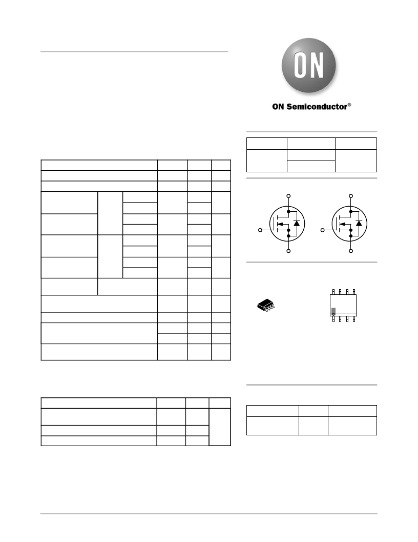
�MARKING� DIAGRAM/�
�PIN� ASSIGNMENT�
�D1� D1� D2� D2�
�8�
�Operating� Junction� and� Storage�
�Temperature�
�Source� Current� (Body� Diode)�
�Single� Pulse� Drain� ?� to� ?� Source� Avalanche�
�Energy� (L� =� 0.1� mH� )�
�T� J� ,� T� STG�
�I� S�
�EAS�
�IAS�
�?� 55� to�
�+150�
�7.0�
�20�
�21�
�°� C�
�A�
�mJ�
�A�
�SO� ?� 8�
�CASE� 751�
�STYLE� 11�
�D5838N�
�AYWW�
�G�
�1�
�S1� G1� S2� G2�
�(Top� View)�
�Lead� Temperature� for� Soldering� Purposes� T� L� 260� °� C�
�(1/8� ″� from� case� for� 10� s)�
�Stresses� exceeding� Maximum� Ratings� may� damage� the� device.� Maximum�
�Ratings� are� stress� ratings� only.� Functional� operation� above� the� Recommended�
�Operating� Conditions� is� not� implied.� Extended� exposure� to� stresses� above� the�
�Recommended� Operating� Conditions� may� affect� device� reliability.�
�A� =� Assembly� Location�
�Y� =� Year�
�WW� =� Work� Week�
�G� =� Pb� ?� Free� Package�
�(Note:� Microdot� may� be� in� either� location)�
�THERMAL� RESISTANCE� MAXIMUM� RATINGS�
�Parameter� Symbol�
�Value�
�Unit�
�ORDERING� INFORMATION�
�Junction� ?� to� ?� Ambient� Steady� State�
�(Notes� 1� &� 3)�
�Junction� ?� to� ?� Ambient� ?� t� ≤� 10� s� (Note� 1)�
�R� q� JA�
�R� q� JA�
�58�
�40�
�°� C/W�
�Device�
�NTMD5838NLR2G�
�Package�
�SO� ?� 8�
�(Pb� ?� Free)�
�Shipping� ?�
�2500/Tape� &� Reel�
�Junction� ?� to� ?� Ambient� Steady� State� (Note� 2)� R� q� JA� 106�
�1.� Surface� ?� mounted� on� FR4� board� using� 1� sq� ?� in� pad�
�(Cu� area� =� 1.127� in� sq� [2� oz]� including� traces).�
�2.� Surface� ?� mounted� on� FR4� board� using� 0.155� in� sq� (100mm� 2� )� pad� size.�
�3.� Both� channels� receive� equivalent� power� dissipation�
�1� W� applied� on� each� channel:� T� J� =� 2� W� *� 58� °� C/W� +� 25� °� C� =� 141� °� C�
�?For� information� on� tape� and� reel� specifications,�
�including� part� orientation� and� tape� sizes,� please�
�refer� to� our� Tape� and� Reel� Packaging� Specification�
�Brochure,� BRD8011/D.�
�?� Semiconductor� Components� Industries,� LLC,� 2012�
�February,� 2012� ?� Rev.� 1�
�1�
�Publication� Order� Number:�
�NTMD5838NL/D�
�发布紧急采购,3分钟左右您将得到回复。
相关PDF资料
NTMD6N02R2
MOSFET PWR N-CH DL 3.92A 20V 8SO
NTMD6N03R2
MOSFET PWR N-CH DL 6A 30V 8SOIC
NTMD6P02R2G
MOSFET PWR P-CHAN DUAL 20V 8SOIC
NTMFD4901NFT1G
MOSFET N-CH DUAL 30V 8DFN
NTMFS4108NT1G
MOSFET N-CHAN 22A 30V SO-8FL
NTMFS4119NT1G
MOSFET N-CHAN 18A 30V SO-8FL
NTMFS4120NT1G
MOSFET N-CHAN 18A 30V SO-8FL
NTMFS4121NT1G
MOSFET N-CHAN 17A 30V SO-8FL
相关代理商/技术参数
NTMD6601NR2G
功能描述:MOSFET NFET S08D 80V 1.4A 245mOHM RoHS:否 制造商:STMicroelectronics 晶体管极性:N-Channel 汲极/源极击穿电压:650 V 闸/源击穿电压:25 V 漏极连续电流:130 A 电阻汲极/源极 RDS(导通):0.014 Ohms 配置:Single 最大工作温度: 安装风格:Through Hole 封装 / 箱体:Max247 封装:Tube
NTMD6N02R2
功能描述:MOSFET 20V 6A N-Channel RoHS:否 制造商:STMicroelectronics 晶体管极性:N-Channel 汲极/源极击穿电压:650 V 闸/源击穿电压:25 V 漏极连续电流:130 A 电阻汲极/源极 RDS(导通):0.014 Ohms 配置:Single 最大工作温度: 安装风格:Through Hole 封装 / 箱体:Max247 封装:Tube
NTMD6N02R2/D
制造商:未知厂家 制造商全称:未知厂家 功能描述:Power MOSFET 6.0 Amps, 20 Volts
NTMD6N02R2_05
制造商:ONSEMI 制造商全称:ON Semiconductor 功能描述:Power MOSFET 6.0 Amps, 20 Volts
NTMD6N02R2G
功能描述:MOSFET NFET 20V 0.035R TR RoHS:否 制造商:STMicroelectronics 晶体管极性:N-Channel 汲极/源极击穿电压:650 V 闸/源击穿电压:25 V 漏极连续电流:130 A 电阻汲极/源极 RDS(导通):0.014 Ohms 配置:Single 最大工作温度: 安装风格:Through Hole 封装 / 箱体:Max247 封装:Tube
NTMD6N03R2
功能描述:MOSFET 30V 6A N-Channel RoHS:否 制造商:STMicroelectronics 晶体管极性:N-Channel 汲极/源极击穿电压:650 V 闸/源击穿电压:25 V 漏极连续电流:130 A 电阻汲极/源极 RDS(导通):0.014 Ohms 配置:Single 最大工作温度: 安装风格:Through Hole 封装 / 箱体:Max247 封装:Tube
NTMD6N03R2G
功能描述:MOSFET NFET 30V SPCL TR RoHS:否 制造商:STMicroelectronics 晶体管极性:N-Channel 汲极/源极击穿电压:650 V 闸/源击穿电压:25 V 漏极连续电流:130 A 电阻汲极/源极 RDS(导通):0.014 Ohms 配置:Single 最大工作温度: 安装风格:Through Hole 封装 / 箱体:Max247 封装:Tube
NTMD6N04R2
制造商:ONSEMI 制造商全称:ON Semiconductor 功能描述:Power MOSFET 40 V, 5.8 A, Dual N-Channel SOIC-8